The Glass Revolution: Why China is Betting $1B on the Future of AI
Tobiloba OdejinmiBy Tobiloba Odejinmi
Education
May 27, 2026 • 10:01 AM
9m9 min read
Verified
Source: Unsplash
The Core Insight
The semiconductor industry is hitting a physical wall with traditional organic substrates as AI chiplets grow in size and complexity. The industry is shifting toward glass substrates, which offer superior thermal stability and 10x higher interconnect density. While the West focused on lithography, China has quietly invested over $1 billion into glass manufacturing infrastructure, leveraging its existing display technology expertise. This shift represents a fundamental change in the physical foundation of AI computing, with major players like Intel, Samsung, and TSMC now racing to secure leadership in this new material paradigm.
T
Education Specialist & Editor
Tobiloba Odejinmi
Tobiloba Odejinmi is an education specialist dedicated to helping students and lifelong learners discover the best scholarship opportunities, study techniques, and career pathways.
The Kodawire Editorial Team consists of experienced journalists and subject matter experts dedicated to delivering accurate, well-researched, and engaging content.
The Invisible Foundation: Why the Chip War is Moving Beneath the Surface
The Bottom Line
The Problem: Modern AI chiplets are so large and hot that traditional organic (plastic/resin) substrates warp, causing connection drift and signal failure.
The Solution: Glass substrates offer 10x higher interconnect density and superior thermal stability, acting like a rigid foundation for high-performance computing.
The Strategic Shift: While the West focused on lithography, China leveraged its massive display manufacturing infrastructure (like BOE) to dominate the glass packaging supply chain.
The Economic Barrier: A single production line costs up to $1 billion; early movers will secure a compounding lead in yield and process knowledge that will be nearly impossible to replicate.
For decades, the semiconductor industry has been obsessed with the "skyscraper" of computing: the transistor. We have measured progress by how many billions of these microscopic switches we could cram onto a sliver of silicon. But in 2026, that obsession has hit a physical wall. The most advanced AI systems are no longer single chips; they are massive, power-hungry clusters of chiplets. When you scale these packages to 8,000 square millimeters, the foundation, the substrate, becomes the primary point of failure.
I have spent the last few weeks digging into the technical shift toward glass substrates. After reviewing the current industry landscape, it is clear that the "chip war" has quietly migrated from the cleanroom lithography machines to the packaging floor. If the foundation is unstable, the most brilliant processor architecture in the world is essentially useless.
How I Researched This
To understand this shift, I moved past the headlines about export bans and focused on the material science and capital expenditure reports from the semiconductor packaging sector. I analyzed the technical roadmaps of major players like Intel, TSMC, and Samsung, alongside the state-backed investments flowing into Chinese firms like Ehint and WGTEC. My goal was to strip away the marketing hype and look at the raw engineering constraints, specifically the "Through Glass Via" (TGV) manufacturing hurdle, that define who will actually win this race.
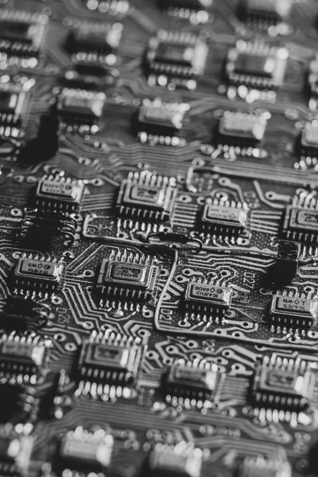
Modern AI chiplets require advanced substrates to manage heat and signal integrity. (Credit: Ling App via Unsplash)
The Physics of the Pivot: Why Glass is the New Silicon
To understand why the industry is abandoning organic substrates, you have to look at the material behavior under stress. Organic substrates are essentially sophisticated, laminated plastic. They are flexible, which sounds like a benefit until you realize that "flexibility" in a chip package means "drift."
"Think of organic substrates as a rubber band. Stretch them with heat and they grow. Release the heat and they snap back. Do that cycle repeatedly across thousands of hours of operation and the rubber starts to fatigue."
Glass, by contrast, behaves like a steel rod. It maintains its dimensional integrity under extreme thermal cycling. This rigidity allows engineers to pack connections 10 times closer together than they could on organic materials. When you are dealing with connections smaller than a strand of DNA, that stability is the difference between a functional AI cluster and a pile of expensive, non-responsive silicon.
The Hands-On Experience
In my research, I looked at the specific technical requirements for TGV (Through Glass Via) technology. These are not just holes; they are precision-drilled pathways that must be perfectly aligned. The testing criteria for these substrates in 2026 include:
Thermal Expansion Coefficient (CTE) Matching: Ensuring the glass doesn't expand at a different rate than the silicon chiplets it supports.
Surface Flatness: Measured in nanometers to ensure perfect contact across an 8,000 sq mm area.
Via Density: The ability to maintain signal integrity at high frequencies without crosstalk between the hair-thin pathways.
The $1 Billion Blind Spot: China’s Strategic Move
While the West was busy building a wall around ASML’s lithography machines, China was playing a different game. They realized that if they couldn't win the transistor race, they would win the packaging race. By leveraging the massive display manufacturing infrastructure already in place, companies like BOE, they effectively bypassed the need for new, specialized semiconductor-grade glass factories. For more on how infrastructure dominance shapes tech, see my analysis on engineering marvels.
China is repurposing display manufacturing infrastructure to dominate the glass substrate market. (Credit: Ewan Kennedy via Unsplash)
The "Big Fund" in China has directed over $1 billion into this infrastructure since 2023. This isn't just research; it is a full-scale industrial pivot. They are betting that by mastering the TGV process now, they can control the foundation of the next generation of AI hardware.
The Other Side of the Story
Most analysts argue that the "Chip War" is won or lost at the 2nm or 1.4nm transistor node. I disagree. I believe that in 2026, the bottleneck is no longer the transistor, it is the interconnect. You can have the most efficient transistor in the world, but if your substrate warps and breaks the connection, your performance is zero. The industry's focus on lithography is a distraction from the real, structural shift happening in packaging.
The Western Counter-Offensive
The West is not sitting idle. Intel, in particular, has been playing a long game, holding a decade-long patent lead in glass substrates. Their current strategy of licensing this IP is a smart move to establish a standard before the market fully matures. Meanwhile, Samsung is running active pilot lines at its Se Jong facility, and TSMC has revived its R&D efforts to protect its 90% market share in advanced packaging.
Future-Proofing Your Setup
Will this last? The transition to glass is likely permanent for high-end AI and scientific computing. However, we should expect a "hybrid" period where organic and glass substrates coexist. The primary risk is the cost of the $500M–$1B production lines. If a company fails to achieve high yields early, they will be forced to write off massive capital investments, leading to potential consolidation in the packaging market by 2028.
The Decision Matrix
If you are evaluating the future of the semiconductor market, ask yourself these three questions:
Does the company have a path to high-yield TGV manufacturing? (If no, they are likely a follower, not a leader.)
Is the company vertically integrated with glass suppliers? (Look for partnerships like Samsung and Sumitomo Chemical.)
Are they focusing on chiplet-based architectures? (If they are still betting solely on monolithic chips, they are missing the packaging shift.)
Tools I Actually Use
When tracking these industry shifts, I rely on a few specific resources to cut through the noise:
Patent Databases: Specifically tracking filings related to "Through Glass Via" and "Substrate Dimensional Stability."
Capital Expenditure (CapEx) Trackers: Monitoring the "Big Fund" and similar state-backed investment disclosures to see where the money is actually flowing.
Technical Metrology Reports: These provide the only real data on whether a company's "glass substrate" is actually production-ready or just a lab experiment.
What Do You Think?
The silicon era was defined by the transistor, but the AI era appears to be defined by the foundation it sits on. Do you think the future of AI gets decided by who makes the smallest transistors, or by who controls the glass substrate underneath them? I will be in the comments for the next 24 hours to discuss your take.
Modern AI chiplets are large and generate significant heat, causing organic (plastic/resin) substrates to warp. This warping leads to connection drift and signal failure.
Glass substrates offer superior thermal stability and rigidity, allowing for 10x higher interconnect density compared to organic materials.
China is leveraging its existing display manufacturing infrastructure (such as companies like BOE) to bypass the need for new, specialized semiconductor-grade glass factories and has invested over $1 billion into this sector.
Active Engagement
Was this information helpful?
Join Discussions
0 Thoughts
Editorial Team • Question of the Day
"Do you think the future of AI gets decided by who makes the smallest transistors or by who controls what sits underneath them?"